



Smaller, lower-cost semiconductor facilities could widen access to chipmaking, even as mass production remains dominated by industrial giants.
Can we manufacture chips without billion-dollar fabs?
Can we manufacture chips without billion-dollar fabs?
By The Beiruter | October 10, 2026

Reading time: 5 mins
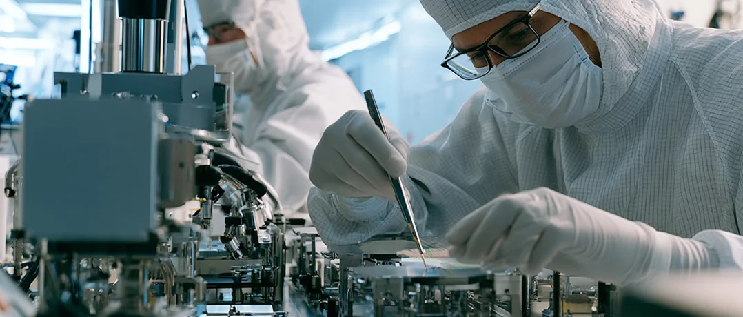
The modern semiconductor industry has become an extraordinary exercise in industrial concentration. The most advanced chips powering smartphones, artificial intelligence, and sophisticated military systems depend on manufacturing facilities that can cost tens of billions of dollars, with leading-edge production concentrated among a small number of companies and countries. Yet researchers are exploring smaller facilities and open-source equipment that could make certain kinds of chip fabrication accessible to universities, startups, and countries without established semiconductor industries. Making a functioning chip, however, is considerably easier than producing millions of them at a competitive price. “In high-volume manufacturing, the reason electronics have gotten cheaper and more powerful for decades is because of the cost,” Larry Pileggi, professor of electrical and computer engineering at Carnegie Mellon University, told The Beiruter. Although smaller-scale fabrication may not replace mass production, it could serve specialized markets and widen access to semiconductor research. The enormous cost of semiconductor manufacturing is not simply a consequence of technological complexity. It is also central to the industry's business model. Modern fabs manufacture chips on circular silicon wafers, carrying out hundreds of tightly controlled processing steps before cutting the wafers into individual devices. Expensive machinery allows manufacturers to process large volumes with exceptional precision, reducing the cost per chip. The industry's financial commitments are still growing. SEMI, the international semiconductor industry association, projected in its 2026 300mm Fab Outlook that spending on equipment for facilities using 300-millimeter wafers would reach $149 billion this year, an increase of 31% over 2025. It expects further growth through 2029, driven partly by demand for artificial intelligence and advanced computing. “Without equipment capable of manufacturing many chips per minute or per hour, it would be impossible to keep up with commercial demand,” Pileggi said. Still, Pileggi explained, not every semiconductor needs to be manufactured in enormous quantities or at the industry's most advanced technological level. Chips used in industrial equipment, sensors and power management have different requirements from advanced AI processors, potentially creating opportunities for smaller facilities producing specialized devices. “One customer would be governments, using chips in military applications where production volumes are relatively low,” he said. At Carnegie Mellon, Pileggi's Hacker Fab initiative has produced functioning transistors with features as small as one micron using student-built equipment for patterning silicon and depositing metals. Its open-source designs allow other institutions to experiment with semiconductor fabrication without relying entirely on expensive commercial machinery. The debate over smaller fabs comes as governments in the United States, Europe, Japan, and elsewhere are committing substantial public resources to expanding domestic semiconductor manufacturing. The concentration of production has become a concern not only for industrial competitiveness but also for economic security. Taiwan remains particularly important. According to TrendForce, a market research firm specializing in the semiconductor industry, Taiwan Semiconductor Manufacturing Company (TSMC) accounted for 72.5% of global contract chipmaking revenue in the second quarter of 2026, compared with 5.9% for Samsung Foundry and 5.4% for China's SMIC. The concentration has encouraged investment in alternative manufacturing locations, including Phoenix in Arizona, Dresden in Germany, and Kumamoto in Japan. Yet the effort to diversify production is proceeding largely through the same capital-intensive model that established the industry's geographic concentration. A 2024 study by the Semiconductor Industry Association (SIA) and Boston Consulting Group projected $2.3 trillion in global wafer fabrication investment between 2024 and 2032, compared with $720 billion during the preceding decade. It forecast that the United States would increase its share of global manufacturing capacity from 10% in 2022 to 14% by 2032, while advanced production would spread to additional locations in Europe and Japan. As governments invest in new facilities, the availability of skilled workers is becoming another constraint on expanding production. “The U.S. had a lot of semiconductor manufacturing expertise, and then all the fabs went offshore,” Pileggi said. As manufacturing moved abroad, software offered American engineering students a more immediate route into lucrative technology careers. Semiconductor fabrication, by comparison, required specialized training and offered fewer obvious entry points. “One of the biggest impediments is not money. It's people,” Pileggi said. The shortage is not exclusively American. According to SEMI, the global semiconductor industry association, the industry would need to fill more than one million additional positions by 2030, while a November 2025 assessment by the European Chips Skills Academy found that nearly 30% of Europe's semiconductor workforce was expected to retire by 2030, with relevant graduate numbers growing by less than 1% annually. Training semiconductor engineers requires practical experience, yet universities in countries without established chip industries often lack the expensive equipment needed to manufacture experimental devices. Smaller-scale fabrication initiatives could help address that problem. Pileggi said universities in India have begun adopting open-source equipment designs, while Carnegie Mellon's campus in Rwanda has expressed interest in establishing its own Hacker Fab. Semiconductor equipment manufacturers also have an interest in expanding this talent pipeline. “They need students who are going to be able to invent new equipment,” Pileggi said. Advanced processors will continue to depend on enormous manufacturing investments, while smaller facilities may find opportunities in research, prototyping and specialized devices. For countries unable to compete with established chipmaking powers, these alternatives could provide a way to develop domestic expertise and participate in the semiconductor industry. Making chips without billion-dollar fabs is already possible. Producing them competitively at the volumes demanded by global electronics markets remains considerably harder.Low-cost production requires a very large, high-throughput facility like a commercial fab.
The economics of scale
Low-volume electronics are often associated with government demand.
The geography of chipmaking
In Taiwan, they can find the people to work in the fabs. In China, they can find people to work in the fabs. Here in the United States, we lack that pool of talent.
The next generation of chipmakers
From that standpoint, the most valuable contribution of smaller-scale semiconductor fabrication initiatives is the next generation of engineers being trained.
-
-

-
The Beiruter
-
